TSMC: CoWoS Wafer Packaging Retains Edge Over Panel Tech for Advanced AI Chips
TSMC's Kevin Zhang clarified that wafer-level CoWoS packaging remains essential for high-performance AI processors, offering superior interconnection density and scalability for up to 58 dies. Despite panel-level technologies promising larger packages and lower costs, they won't soon replace CoWoS, which still has significant development runway, addressing industry misconceptions about future chip assembly.
Key points
- Kevin Zhang, TSMC's senior vice president and deputy co-COO, stated that wafer-level chip packaging like CoWoS will not be immediately superseded by panel-level packaging for advanced AI processors.
- CoWoS technology offers superior interconnection densities and can integrate up to 58 dies within a single package, providing significant scalability for demanding AI solutions.
- While panel-level packaging enables larger package sizes, up to 310mm x 310mm compared to existing 120mm x 150mm, and may offer lower costs, it currently lacks CoWoS's geometric complexity handling.
- TSMC asserts there is substantial "runway left" for developing wafer-level technologies, directly countering a common industry misconception about the imminent transition to panel-based methods.
- This clarification helps define the ongoing development strategy for high-performance chip assembly, emphasizing continued reliance on wafer-level approaches for future massive AI chip packages.
TSMC, a leading semiconductor manufacturer, has clarified its outlook on advanced chip packaging technologies critical for future artificial intelligence processors. Kevin Zhang, the company’s senior vice president of business development and global sales, and deputy co-COO, recently stated that wafer-level packaging methods like CoWoS will not be immediately superseded by emerging panel-level techniques. This statement comes amid a growing industry race to develop sophisticated chip packages capable of housing numerous high-performance dies.
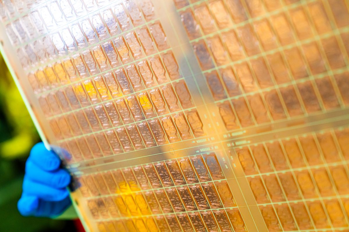
Zhang emphasized that CoWoS (Chip-on-Wafer-on-Substrate) technology offers superior interconnection densities and possesses substantial scalability, capable of integrating up to 58 massive dies within a single package. He highlighted CoWoS's current advantage in handling geometric complexity, asserting that it still has considerable "runway left" for further development and enhancement. This capability is crucial for the demanding requirements of next-generation AI accelerators.
In contrast, while panel-level packaging technologies promise significant advancements, including the potential for much larger package sizes—potentially reaching 310mm x 310mm, a considerable increase from existing 120mm x 150mm—and lower production costs, they currently do not match CoWoS in terms of interconnection density. Zhang addressed a common industry misconception that panel-based solutions would imminently replace wafer-level technologies, indicating that the choice between them depends on specific performance and cost trade-offs.
TSMC’s perspective underscores the continued relevance of wafer-level integration for the highest-performing AI components. This strategic insight helps shape expectations for the semiconductor industry's approach to advanced packaging, signaling that the evolution of AI processors will continue to rely heavily on the sophisticated capabilities offered by established wafer-based methods alongside the gradual development of panel-based alternatives.
Sources
The WireByte editorial team synthesises technology news from multiple primary sources, verifies the facts, and links every source. Articles are produced with AI assistance and reviewed under our editorial policy.